

Powertech to debut world's first panel-level packaging for AI chips by 2027
Taiwan's Powertech plans to mass-produce panel-level packaging for AI chips in 2027, a cost-cutting breakthrough that could challenge TSMC's dominance.

Powertech, a Taiwan-based semiconductor packaging specialist, announced it will be the world's first to mass-produce panel-level packaging (PLP) for AI chips by 2027, targeting a 30% cost reduction over traditional wafer-based methods. This move threatens TSMC's CoWoS packaging monopoly and could reshape the AI chip supply chain, forcing rivals to accelerate their own PLP roadmaps.
Taiwan's Powertech Technology is betting big on a packaging revolution. The company says it will become the first in the world to mass-produce panel-level packaging (PLP) for AI chips by 2027, a move that could slash costs by up to 30% compared to the current wafer-based approach. For an industry scrambling to meet insatiable AI demand, that's not just an incremental improvement-it's a potential game-changer that could redraw the competitive map of advanced semiconductor packaging.
PLP replaces the traditional round silicon wafer with a much larger rectangular panel, typically 510mm by 515mm or even bigger. This simple geometric shift yields dramatically more usable area per production run-roughly 2.5 times the chip output per panel versus a 300mm wafer. Fewer process steps, less material waste, and higher throughput translate directly into lower cost per chip. For AI accelerators, where packaging can account for up to 30% of total manufacturing cost, that's a margin lifeline. Powertech's president, Daniel Ni, told Nikkei Asia that the company has already secured initial customer commitments and is building a dedicated PLP line in its Taiwan facility, with pilot production slated for late 2026 and volume ramp in 2027.
The timing is no accident. AI chip demand has exploded, but the bottleneck isn't just silicon-it's packaging. TSMC's CoWoS (chip-on-wafer-on-substrate) technology, which stacks memory and logic chips on a silicon interposer, is the industry standard for NVIDIA's H100 and AMD's MI300 series. Yet CoWoS capacity has been chronically short, with lead times stretching to over a year. TSMC is spending billions to expand, but its approach remains wafer-based. Powertech's PLP offers a fundamentally different economics: instead of paying premium prices for scarce CoWoS capacity, AI chip designers could turn to a cheaper, higher-volume alternative. That's why Powertech's announcement has sent ripples through the supply chain-and why TSMC is reportedly accelerating its own PLP research, though it has yet to commit to a production timeline.
But Powertech isn't alone in the race. Samsung and Intel have both explored panel-level packaging for years, and Japan's Ibiden and Shinko are developing panel substrates. However, Powertech claims a decisive first-mover advantage: it has already ordered advanced panel lithography and bonding equipment from suppliers like Disco and Tokyo Electron, and it plans to leverage its existing expertise in memory packaging-it's a major supplier for DRAM and NAND modules-to perfect the process. The company's strategy is to target not just AI logic chips but also high-bandwidth memory (HBM) stacks, which are critical components in AI systems. By packaging HBM and logic together on a single panel, Powertech could offer a complete solution that rivals TSMC's integrated CoWoS offering.
The stakes are enormous. The advanced packaging market is projected to grow from $44 billion in 2023 to over $78 billion by 2030, according to Yole Group. TSMC currently controls roughly 60% of the high-end segment, but PLP could erode that dominance. For chip designers like NVIDIA, AMD, and Google, having a second source for advanced packaging is a strategic imperative-it reduces supply chain risk and gives them negotiating leverage. Powertech's move also aligns with broader industry trends toward chiplets and heterogeneous integration, where multiple dies are packaged together. PLP's larger area makes it ideal for assembling many chiplets side by side, enabling more complex and powerful AI processors.
Yet challenges remain. Panel-level packaging has been talked about for over a decade, but technical hurdles have stymied commercialization. Warpage-the bending of the panel during thermal processing-is a notorious problem, as is achieving uniform lithography across a large rectangular surface. Powertech says it has solved these issues through proprietary materials and process controls, but skeptics note that the company has yet to demonstrate yield rates at scale. If yields fall short, the cost advantage evaporates. Moreover, the entire supply chain-from panel substrates to equipment-is still nascent, and Powertech will need to invest billions to build out capacity. The company has not disclosed its total investment, but analysts estimate a full PLP line could cost $500 million to $1 billion.
For executives across the semiconductor ecosystem, Powertech's announcement is a wake-up call. The packaging bottleneck is no longer just a TSMC problem-it's an opportunity. If Powertech delivers on its 2027 timeline, it could become the go-to partner for AI chip companies seeking cost-effective, high-volume packaging. That would force TSMC to either accelerate its own PLP efforts or risk losing share in the fastest-growing segment of the chip industry. It also opens the door for other packaging specialists like ASE and Amkor to follow suit, potentially creating a more fragmented but more competitive landscape. For investors, the key question is whether Powertech can execute. For chip designers, the promise of lower costs and more supply options is a welcome hedge. And for the broader AI economy, cheaper packaging means cheaper AI hardware-which could finally bring down the cost of training and running large models.
In the near term, expect Powertech to face intense scrutiny from industry watchers. The company will need to show pilot results in 2026 to convince customers and investors that its technology is real. If it succeeds, 2027 could mark the beginning of a new era in semiconductor manufacturing-one where the panel, not the wafer, is the unit of production. If it fails, the industry will simply wait for TSMC or Samsung to pick up the mantle. Either way, the race to panel-level packaging is now officially on, and Powertech has fired the starting gun.
This story's Key Insights and Take-aways are locked.
Create a free account to unlock Executive Actions for one credit.
Register to UnlockAlways free for Executives Club members. Join the Club
More in Business

Tim Cook steps down as Apple CEO, stays on as chair with $45M equity
The 'Trump whisperer' keeps his White House and Beijing access as Apple navigates tariffs and a $4.6 trillion market cap.
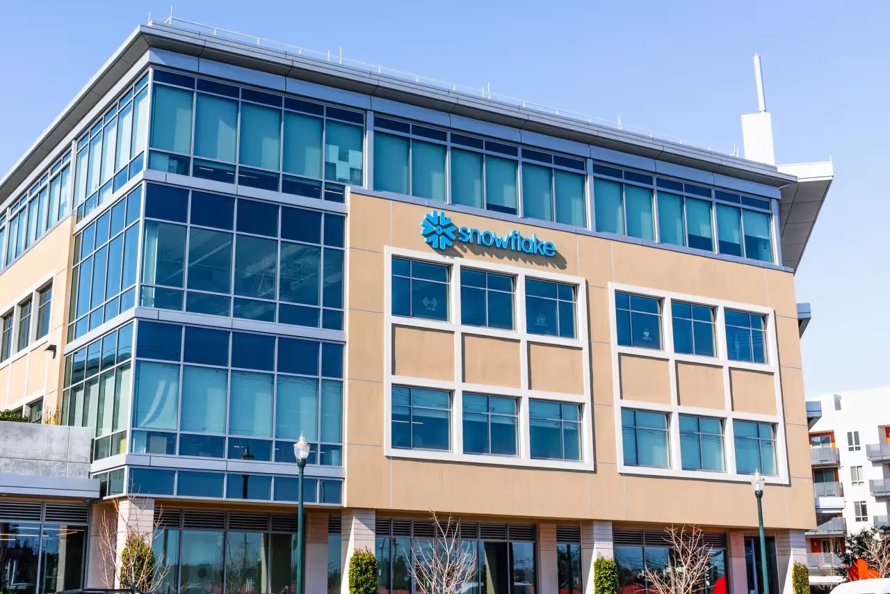
Snowflake shares surge as AI data demand crushes estimates, lifting full-year forecast
Stocks jumped on stronger-than-expected guidance, signaling enterprise AI workloads are accelerating faster than Wall Street priced in.

Tim Cook's 15-year Apple CEO run ends: 3 lessons for any successor
After 15 years, Tim Cook hands Apple to John Ternus - here's how he turned a $350B company into a $4.6T juggernaut.