
A million crystals on a 2cm chip: the new map of how semiconductors split
Perovskites and perovskitoids decide what light they absorb and emit based on their ingredients and internal structure, and a chip just 2 centimeters wide now packs roughly a million crystals that show those mixtures separating into distinct cores and shells.

Researchers working with perovskites and related perovskitoid semiconductors have shown that a chip just 2 centimeters across can hold roughly a million tiny crystals, a miniature material library that reveals how some mixtures separate into distinct cores and shells. For decision-makers in solar, LED and light-detector supply chains, that is a screening tool that could compress the slowest part of materials development, the search for the right recipe.
The number is one million, and the container is roughly the size of a fingernail. A chip just 2 centimeters across can hold about a million tiny crystals, which turns a single small sliver of material into a miniature library of experiments running in parallel. The materials inside that library are perovskites and a related family called perovskitoids, both of them promising semiconductor candidates for solar cells, LEDs and light detectors. Their appeal and their difficulty come from the same place: the ingredients and the internal crystal structure determine how they absorb and emit light, so a small change in the mix can produce a materially different device.
What the chip actually captures is separation. Some mixtures, it shows, do not stay uniform. They resolve into distinct cores and shells, and that internal architecture changes the light they absorb. The plain-English version: think of a coated candy, one substance at the center and a different one wrapped around it. In semiconductor nanocrystals generally, the core typically governs much of the optical behavior while the surrounding shell governs the surface, the part that touches the outside world. That surface is where a lot of real-world performance is won or lost, because it is the boundary that meets moisture, heat and oxygen. A tool that lets researchers see which recipes form cores and shells, and which stay blended, is a tool for controlling a material rather than just discovering it.
Why does a million crystals matter more than one good one? Because a single crystal is a single data point, and materials science has always been bottlenecked by how few data points you can afford. One chip at a million crystals is a million chances to map composition onto structure onto the color of light absorbed. That is the logic behind combinatorial materials research, the long-running idea that you should test many variations at once instead of grinding through them one at a time. Historically, that approach has paid off in fields like pharmaceutical discovery and catalyst development, where broad screening narrows a vast space of possible formulas down to a shortlist worth studying closely. Doing the same for light-emitting and light-absorbing semiconductors is the ambition here, and the 2-centimeter format is what makes it practical rather than theoretical.
The commercial pull is easy to see. Perovskites have been one of the most closely watched families in solar research because they can be processed from solution rather than grown at high temperature, which historically points toward cheaper manufacturing, and because their light absorption can be tuned by changing their chemistry. Lab efficiencies for perovskite solar cells have climbed from low single digits to levels that put them in conversation with established silicon, and the most-discussed near-term application is tandem cells, where a perovskite layer sits on top of silicon to capture more of the solar spectrum. The persistent catch has been durability. These materials are famously sensitive to moisture, heat and light, which is why so much of the field's effort goes into packaging, additives and interface engineering. Anything that clarifies how internal structure drives stability is not a side quest; it is the main quest.
That is where the core-and-shell finding earns its keep. A shell is not decoration. It is a wrapper that can protect a sensitive core, passivate defects at the surface, and shift the wavelength of light a crystal emits. Those are exactly the levers used in commercial light emitters, where nanocrystals with engineered shells already appear in display technology, and they are the levers that matter for LEDs, lasers and photodetectors. If a mixture's tendency to form cores and shells can be read off a chip rather than inferred through painstaking one-off synthesis, teams get to ask better questions earlier: which compositions self-assemble into the architecture I want, and which ones quietly fall apart into something useless?
There is a second-order effect that matters as much as the chemistry. A million-crystal chip is a data-generation machine, and the bottleneck in modern materials discovery is increasingly the dataset rather than the idea. Teams that can produce structured, comparable measurements at that scale build a proprietary map of a composition space, and maps are defensible. That has implications for intellectual property strategy, for how research partnerships are structured, and for the machine-learning groups that need large, clean experimental corpora to train models on. The equipment angle is real too: spotting, printing and reading arrays of tiny crystals is its own engineering discipline, and the labs that get good at it tend to set the tempo for everyone else.
Now the honest caveats. A miniature material library is a characterization and screening advance, not a factory. Showing that mixtures separate into cores and shells tells you what a recipe does; it does not by itself prove that the resulting material survives 25 years on a roof or that it can be coated onto square meters of glass at speed. The gap between a beautiful 2-centimeter chip and a production line is where most promising materials quietly die. But it is also where the cost of failure is lowest, and that is the strategic point. When screening gets a million times denser, the expensive mistakes happen earlier and cheaper, and the shortlist that reaches pilot production is better vetted. For anyone allocating R&D budget in solar, lighting, imaging or displays, the question worth asking is not whether this specific chip changes the roadmap tomorrow. It is whether your organization has access to that kind of high-throughput structural data at all, because the competitors who do will find the winning formulation first, and they will know why it works.
This story's Key Insights and Take-aways are locked.
Create a free account to unlock Executive Actions for one credit.
Register to UnlockAlways free for Executives Club members. Join the Club
More in Science

Anthropic's I.P.O. Made Rank-and-File Researchers Worth Tens of Millions
Researchers who joined just a few years ago are now worth tens of millions, and the windfall resets the pay benchmark for every private A.I. lab still paying in paper.
Sea Lion Culling Strategy Fails: New Model Says Killing Them Won't Save Salmon
The latest research from AAAS overturn a long-held conservation assumption, forcing policymakers to rethink critical resource allocation in marine ecosystems.
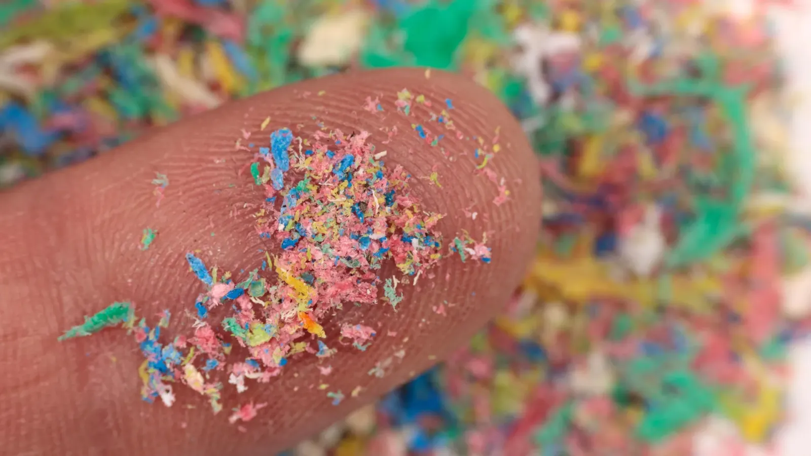
Microplastics do more than pile up: they react with water to damage cells
Scientists have found that plastic particles can generate highly reactive molecules in water, a mechanism that could explain links to heart attacks, strokes, and neurological disorders.